
Intel's 14A node cuts defects faster than any process since 22nm as customers shift from data to capacity.
Intel's 14A node cuts defects faster than any process since 22nm as customers shift from data to capacity.
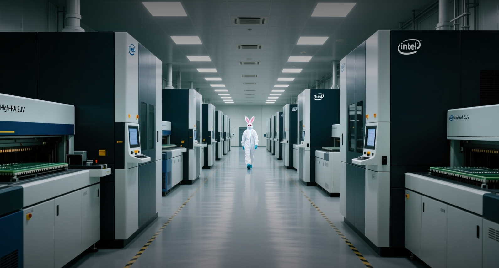
Intel's 14A (1.4nm-class) process node is cutting defect density faster than any node since 22nm, with external foundry customers shifting from data review to capacity allocation questions, CFO David Zinsner said.
"When you look at the defect density, 14A is tracking better than the target curve we had for 14A," Zinsner said at Deutsche Bank's 2026 Technology Conference on Aug. 26. "It is also doing better than any of the previous nodes in terms of how quickly we are bringing down the defects. In fact, we have not seen this performance since 22nm."
14A pairs second-generation gate-all-around RibbonFET transistors with PowerDirect backside power delivery and High-NA EUV lithography. Intel projects 15-20 percent higher performance at the same power versus 18A, or 25-35 percent lower power at the same performance, with up to 30 percent higher chip density. Risk production for internal products begins in the second half of 2027, with mass production in 2028.
The progress matters for Intel Foundry's economics. The division posted external revenue of $293 million and an operating loss of $2.089 billion in Q2 2026. Intel's 2025 Form 10-K states that leading-edge node economics require wafer volumes beyond Intel's own products, and the company has noted the possibility of discontinuing subsequent nodes if it fails to secure external customers for 14A.
The 22nm comparison carries weight because that node marked Intel's last period of unambiguous manufacturing leadership. Intel's 22nm process, which entered volume production in late 2011 and launched commercially with Ivy Bridge in April 2012, was the industry's first FinFET (three-dimensional transistor) node. Competitors did not match it until their 14nm and 16nm nodes in 2014-2015, a gap of more than two years. The post-22nm era brought a 14nm delay, a failed 10nm node, the cancellation of 20A, and elevated defect density on 18A even as it reached high-volume manufacturing.
The comparison has limits. Zinsner was comparing 14A's defect reduction trajectory at roughly two years before mass production to where 22nm stood at a comparable point in 2010 — not the absolute defect levels of the two nodes. Inspection equipment has improved substantially in 16 years, meaning what Intel counts as a defect today may differ from what it counted in 2010. Defect density also does not directly translate to product yield, which depends on die area, circuit redundancy, and voltage-frequency specifications.
Customer conversations shift from data to supply
The more commercially significant signal is the change in external customer engagement. CEO Lip-Bu Tan and his team now meet with foundry customers weekly, Zinsner said, and discussions have moved from reviewing process data to questions about capacity and supply. Tesla is the only publicly confirmed external 14A customer, announced in April for its Terafab project in Austin, Texas. Nvidia, AMD, Apple, and Broadcom have been reported as evaluating 14A or Intel's EMIB packaging, though none has confirmed a production commitment.
The Process Design Kit 0.9 release, targeted for October 2026, opens the formal design cycle. PDK 0.5 is already distributed to lead customers. A customer receiving PDK 0.9 in October could begin production-intent tape-out cycles in late 2026 or early 2027, positioning their chips for Intel's risk production schedule in the second half of 2027.
Competitive positioning vs TSMC
Intel's 14A is designed around ASML's High-NA EUV scanners, which cost $380 million per unit. Intel was the first manufacturer to ship High-NA EUV logic chips, on 18A in 2026. TSMC's CEO stated in April 2026 that the company sees no need for High-NA EUV through its 2029 roadmap, giving Intel a potential 18-to-24-month learning advantage. On backside power delivery, 14A's PowerDirect is two generations ahead of TSMC's current production nodes — TSMC's first backside-powered node, A16, is targeted for late 2026.
Intel also highlighted EMIB-T, its packaging technology competing with TSMC's CoWoS. Zinsner projected EMIB-T could become a business worth multiple billions of dollars per customer per year, with gross margins around 40 percent and operating margins around 30 percent. Revenue is expected to begin ramping in the second half of 2027.
Intel shares have been volatile as investors weigh the foundry turnaround against the capital intensity of leading-edge manufacturing. The 14A defect trajectory is a positive signal, but mass production is two years away, and the company has not disclosed absolute D0 values, product names, or signed external capacity contracts. Intel Foundry's Q2 operating loss of $2.089 billion shows the financial stakes: the division needs external wafer volumes to make leading-edge economics work.
This article is for informational purposes only and does not constitute investment advice.
