


Intel's EMIB-T advanced packaging ramp targets a market where TSMC's CoWoS holds yields above 98 percent on 5.5x reticle designs.
Intel's EMIB-T advanced packaging ramp targets a market where TSMC's CoWoS holds yields above 98 percent on 5.5x reticle designs.
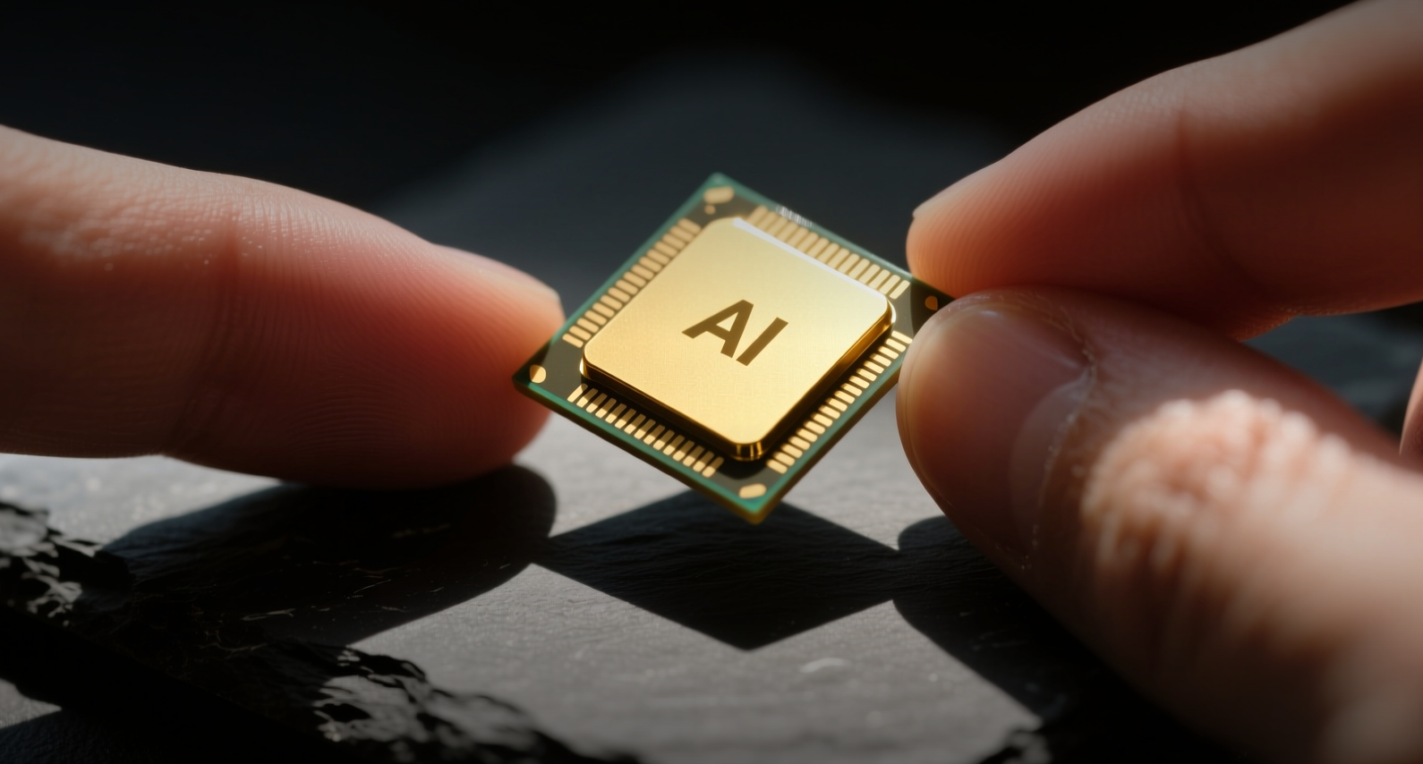
Intel is accelerating its EMIB-T advanced packaging ramp to challenge TSMC's CoWoS in a market projected to grow from $46.1 billion to $79.4 billion by 2030, as AI demand for processor-memory links intensifies.
"We are now focused on ramping EMIB-T into high-volume production to support customer ramps in 2027," Intel CEO Lip-Bu Tan said on the company's Q2 2026 earnings call.
Intel's EMIB-T is expected to scale beyond 8x reticle size this year and exceed 12x by 2028. TSMC's CoWoS, in volume production at 5.5x reticle size with yields consistently above 98 percent, plans to scale beyond 14x by 2029. Intel's approach embeds a silicon bridge directly into the substrate, eliminating the full-size interposer that CoWoS requires — a design that lowers cost by removing the interposer layer.
The stakes are substantial. Counterpoint Research estimates more than 130 million GPUs and AI ASICs will ship with advanced-packaged on-compute memory over the next five years, generating nearly $2 trillion in compute revenue. Intel's foundry business posted $5.8 billion in Q2 revenue, up 31 percent year over year, but the company trades at 66x forward earnings after a 400 percent stock surge over the past year.
As semiconductor nodes shrink toward 2nm and beyond, the industry has shifted from planar transistors to FinFET and now GAAFET architectures. But process scaling costs continue to climb, pushing chip designers toward disaggregation — splitting a single die into multiple chiplets connected through advanced packaging. The interconnect quality between dies determines whether a chiplet design delivers on its promise of high-bandwidth, low-latency communication.
TSMC's CoWoS (Chip-on-Wafer-on-Substrate) integrates multiple dies onto a silicon interposer via micro-bumps, then bonds the interposer to the package substrate. The approach has become the de facto standard for AI accelerators, with Nvidia, AMD and major cloud providers relying on it for HBM integration. TSMC holds roughly 72 percent of the global foundry market, according to TrendForce.
Intel's EMIB (Embedded Multi-die Interconnect Bridge) takes a different path. Instead of a full-size interposer, it embeds a silicon bridge directly into the substrate to serve as the communication link between chips. This reduces material costs and simplifies the manufacturing flow. The company has also partnered with SoftBank's SAIMEMORY on ZAM, a near-to-mid-term HBM4-class memory interface challenger, and is developing XBM, a longer-term redesign using BEOL thin-film transistors and serial UCIe.
Taiwan's OSAT providers are also moving. ASE's Fan-Out Chip on Substrate (FOCoS) uses multiple redistribution layers to integrate processors, memory and I/O chips, delivering interconnect density roughly 50x that of traditional flip-chip packaging — and over 200x with FOCoS-Bridge. SPIL has developed FOEB (Fan-Out Embedded Bridge), embedding silicon bridges within the RDL layer for near-monolithic, high-density connections between dies.
The advanced packaging market is growing at roughly 9.5 percent annually, according to Yole Group data cited by SEMI, with 3D stacking and hybrid bonding growing at about 25 percent per year between 2023 and 2029, per TechInsights. That growth is concentrated in AI-linked technologies: HBM stacking, 2.5D/3D integration, and co-packaged optics.
Intel's foundry business has momentum beyond packaging. The company recently landed Fortinet as a customer for its Security Processor 6, manufactured on the Intel 4 node — the first named outside customer under Tan's leadership. Foundry revenue grew 31 percent in Q2 to $5.8 billion, above the company's 25 percent target.
Intel shares have surged 400 percent over the past year, leaving the stock at 66x forward earnings. The market has already priced in substantial foundry turnaround expectations. TSMC, by contrast, maintains a significant scale and technology advantage in advanced packaging, with CoWoS yields topping 98 percent across multiple AI customer products.
The question for investors is whether Intel's EMIB-T can close the gap by 2027, when Tan expects high-volume production to support customer ramps. If Intel delivers on that timeline, it could pressure TSMC's pricing power in the AI packaging segment. If not, TSMC's entrenched position — backed by JEDEC-standard compatibility and proven manufacturing scale — will likely hold.
This article is for informational purposes only and does not constitute investment advice.
